


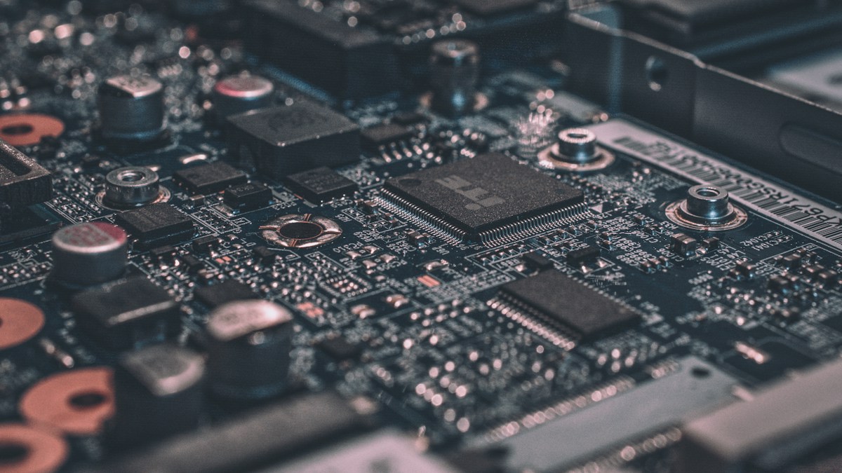
For years, the global conversation surrounding semiconductor sovereignty focused almost exclusively on nanometer gate geometries and extreme ultraviolet (EUV) lithography scanners.
However, as physical transistor scaling approaches quantum limits, the competitive frontier of computing power has shifted decisively to advanced packaging—the intricate engineering required to bind silicon chiplets, logic dies, and high-bandwidth memory stacks into a single multi-terabyte processor.
Recognizing that advanced packaging has become the acute supply chokepoint for artificial intelligence hardware, major foundries are establishing high-throughput packaging fabs in Japan, the United States, and Europe, redistributing the critical links of global silicon assembly.
"Packaging is no longer a downstream assembly function; it is the core determinant of chip performance and geopolitical supply resilience."— Semiconductor Industry Association Global Supply Report
HBM4 Integration and Geopolitical Resilience
The newest facilities are engineered to handle next-generation HBM4 memory architectures utilizing sub-micron hybrid bonding techniques. By establishing packaging nodes across allied territories, chip designers can insulate customer delivery schedules against regional geopolitical shocks.


Inquiries and discussions must maintain diplomatic civility, analytical depth, and factual accuracy.
Sign in with your Google account to contribute to diplomatic discussions
No reader commentary yet
Be the first verified reader to submit your diplomatic dispatch or critique.